Colloidal Silicon Nanocrystals
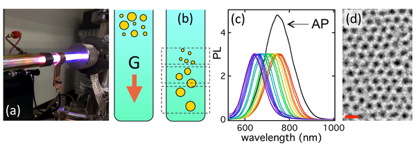
Our group synthesizes colloidal silicon nanocrystals (SiNCs) at NDSU using a variety of techniques, including nonthermal plasmas [(a), NDSU reactor]. We passivate the SiNCs using a number of different surface chemistries, which makes the nanocrystals colloidally stable in organic solvents while enhancing their optical properties. We then purify the SiNCs by size (b) to study their photophysics (c) and self-assembly into ordered 'superlattices' [(d), 10 nm scale]. We are mainly interested in SiNC photo-luminescence (PL), including PL quantum yield and PL lifetime, and how the PL is impacted by nanocrystal size, surface chemistry, and the environment.
Colloidal Perovskite Nanocrystals
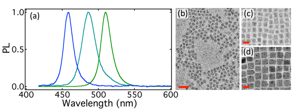
In addition to silicon, we also study lead-halide perovskite (LHP) nanocrystals. Panel (a) shows three different sizes of colloidal LHP nanocrystals synthesized by our group, where the PL emission spans blue to green. The nanocrystals can be made in a variety of different sizes [(b), 20 nm scale, (c) 10 nm scale, (d) 10 nm scale], each corresponding to a different color and intensity of PL. We use variations in LHP chemistry to produce particles with emission in the red, orange and yellow. Again, we are primarily interested in PL (spectra, quantum yield, lifetime and stability) and self-assembly into ordered super-lattices [(c) & (d)], where the latter is constrained by the unique cubic shape of the nanocrystals. As with silicon, we also make functional polymer-nanocomposite thin films using a variety of different polymer chemistries.
Single-Wall Carbon Nanotube (SWCNT) Solar Cells
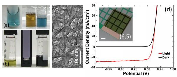
Starting from colloidal single-wall carbon nanotubes (SWCNTs) of varied purity, chirality, and electronic type (metallic vs. semiconducting) [(a) & (b)], we assemble multi-functional thin (10 to 100 nm thick) SWCNT films through vacuum filtration (c). We then dope these SWCNT films and use them to make flexible transparent conductive layers and SWCNT-silicon heterojunctions (d), where we are primarily interested in the chemical structure of the junction interface. For example, we recently demonstrated that metallic SWCNT films can form an effective p-n junction with n-type silicon, where the SWCNT layer acts in a manner similar to a heavily doped semiconductor. Without additional surface treatment, such as anti-reflective coating, these devices typically have photoconversion efficiencies of around 10-13 %.
Extreme Mechanics of Multifunctional Nanosheets
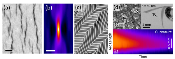
Freestanding multifunctional nanosheets have a number of potential applications in flexible electronics. To study the mechanics of such films, we process them as freestanding nanosheets and deposit them on PDMS substrates, for example, which we then compress to measure how the sheet topography develops under strain [(a) & (b)]. The response if often very different from that observed for thin polymer films (c) but can still provide information about nanosheet stiffness and durability. To obtain additional information about the mechanics of these films, we also suspend the freestanding nanosheets in simple solvents such as ethanol (d) and measure the relaxation of nanosheet curvature (bottom) back to equilibrium following a controlled deformation.
This Web page represents the views of the author and not necessarily those of North Dakota State University.
NDSU is not responsible or liable for its contents.